Power Electronic
Introduction
The tunnel diode is that the contact device that exhibits negative resistance. which means once the voltage has accumulated the present through it decreases. Classically, a carrier should have the energy a minimum of adequate to potential-barrier height to cross the junction.But consistent with quantum physics, there’s the finite likelihood that it will penetrate through the barrier for a skinny breadth. This development is termed tunneling and thus the physicist Diode is thought as Tunnel Diode.
Electron Tunneling in the p-n junction
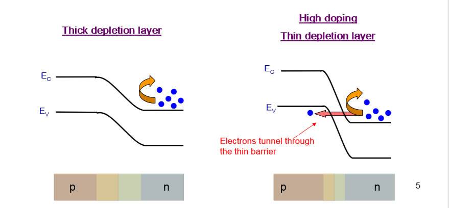
- When the p and n region is extremely doped, the depletion region becomes terribly skinny (~10nm).
- In such case, there’s a finite likelihood that electrons will tunnel from the physical phenomenon band of n-region to the valence band of p-region.
- During the tunneling, the particle ENERGY doesn’t an amendment
Components:
01.Tunnel Diode: [ See Buy Click Amazon ]
Tunnel Diode Operation
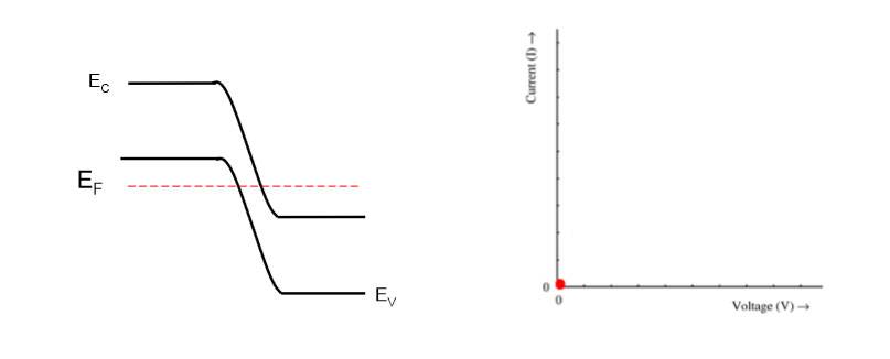
When the semiconductor is incredibly extremely doped (the doping is bigger than No) the Fermi level goes higher than the conductivity band for n-type and below valence band for p-type material. This square measure is known as degenerate materials.
Under
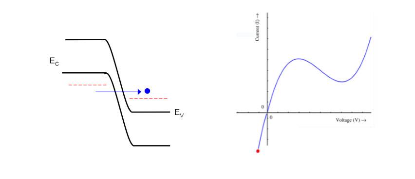
Step 1: At zero bias there is no current flow
Step 2: A small forward bias is applied. Potential barrier continues to be terribly high – no noticeable injection and forward current through the junction. However, electrons within the physical phenomenon band of the n region can tunnel to the empty states of the valence band in p region. this may produce a forward bias tunnel current.
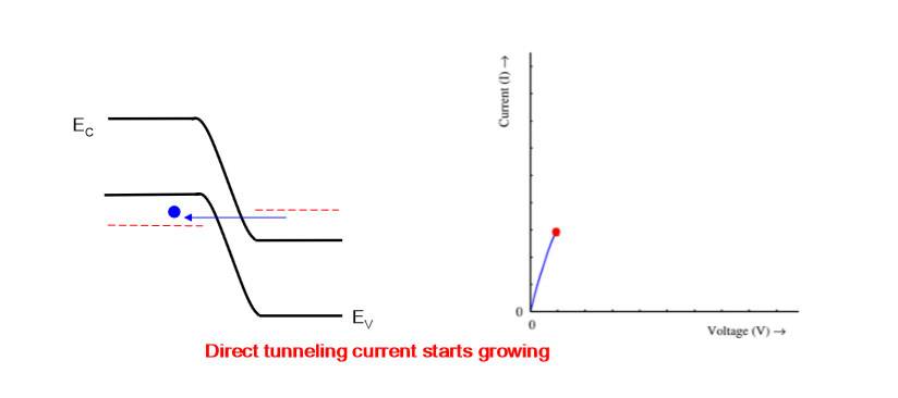
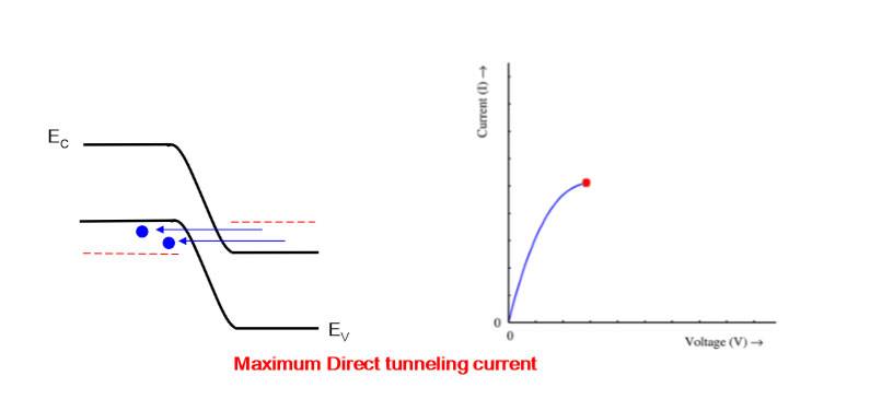
Step 3: With a bigger voltage the energy of the bulk of electrons within the n-region is adequate to that of the empty states (holes) within the valence band of p-region; this may manufacture most tunneling current.
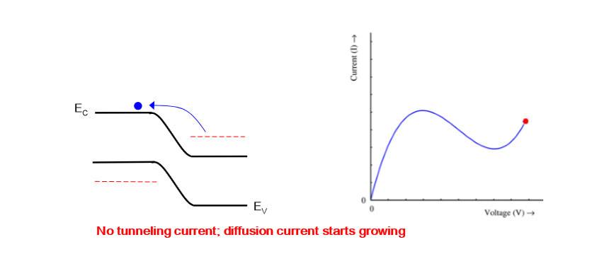
Step 4: As the forward bias continues to extend, the number of electrons within the n aspect that area unit directly opposite to the empty states within the valence band (in terms of their energy) decrease. so decrease within the tunneling current can begin.
Step 5: As a lot of forwarding voltage is applied, the tunneling current drops to zero. however, the regular diode forwards current because of electron-hole injection will increase because of a lower potential barrier.
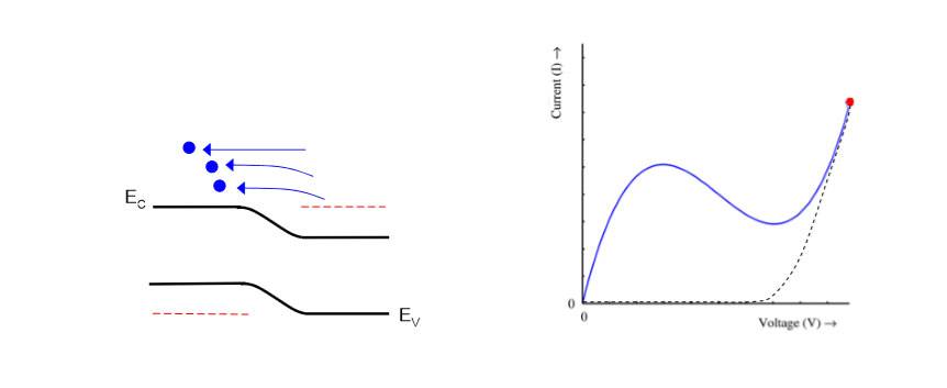
Step 6: With further voltage increase, the tunnel diode I-V characteristic is similar to that of a regular p-n diode.
Tunnel Diode Operation
Under Reverse Bias
In this case the, electrons within the valence band of the p facet tunnel directly towards the gift of the empty state within the physical phenomenon band of the n facet making massive tunneling current that will increase with the appliance of reverse voltage. The TD reverse I-V is comparable to the Zener diode with nearly zero breakdown voltage.