Introduction to Transistor
Transistors make our electronics world go ’round. They’re critical as an impact source in only about every modern circuit. Sometimes you see them, but more-often-than-not they’re hidden deep within the die of a microcircuit. during this tutorial, we’ll introduce you to the fundamentals of the foremost common transistor round the bipolar transistor (BJT).
The transistor might be a semiconductor device that can conduct and insulate at the same time. A transistor has switch and amplifier capabilities. It controls electronic currents by converting audio waves into electronic waves and resistors. Germanium was used in the manufacturing of the main transistor. A transistor serves the same purpose as a tube triode, except instead of heating electrodes in a chamber, it uses semiconductor junctions. It is the fundamental component and may be found everywhere in contemporary electronic systems.
Different Types of Transistors
There are two different types of transistors: field-effect transistors (FET) and bipolar junction transistors (BJT). The base terminal can control a larger current flow between the collector and the emitter terminals when just a small amount of current is flowing between the bottom and the emitter. A voltage at the gate of a FET can control the current flowing between the source and drain. A FET also has three terminals: the gate, source, and drain. The simple diagrams of the BJT and FET are displayed in the following figure:
Bipolar Junction Transistor
Field Effect Transistor
01. Bipolar Junction Transistor:
Three terminals coupled to three doped semiconductor areas make up a bipolar transistor (BJT). It is available in the N-P-N and P-N-P forms.
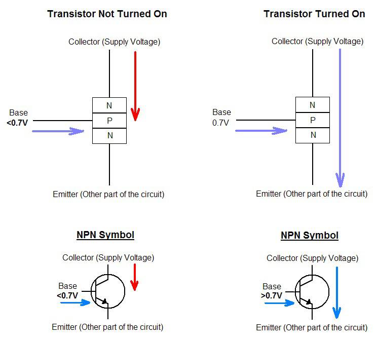
A P-doped semiconductor layer is sandwiched between two layers of N-doped material to form an N-P-N transistor. We obtain the high collector and emitter current by amplifying the bottom current.
When the base of the NPN transistor is pulled low in relation to the emitter, the transistor is ON. The transistor’s collector and emitter are where the current flows when the transistor is turned on. the electrons traveling from the emitter to the collector were supported by tiny minority carriers within the P-type region. Since it enables higher current and quicker operation, NPN bipolar transistors are the most common type of bipolar transistor used today.
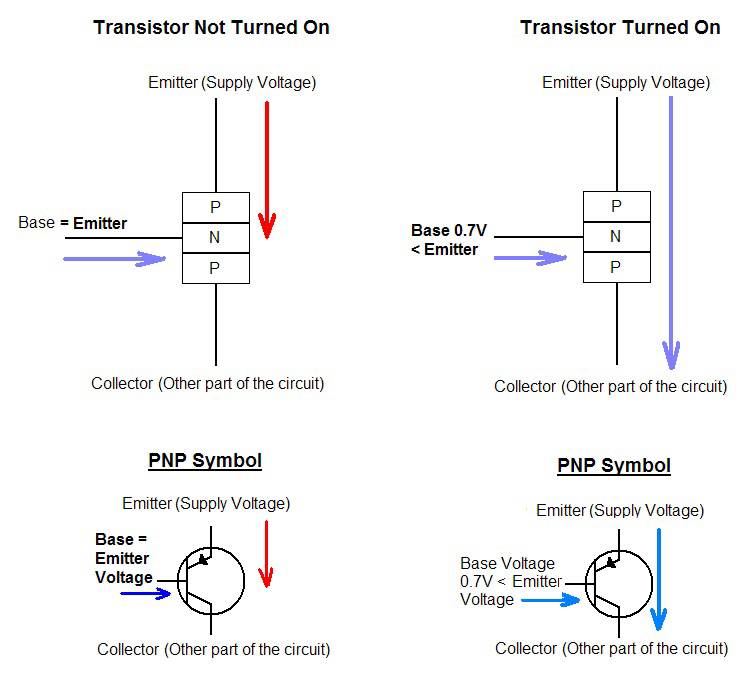
P-N-P transistor has two layers of P-doped material sandwiching an N-doped semiconductor layer. At the collector’s output, the bottom current is amplified.
When the base of the PNP transistor is pulled low in relation to the emitter, the transistor turns ON. When the PNP transistor is operating in forward active mode, the arrows on the device represent the direction of current flow.
02. Field Effect Transistor (FET):
N-channel or P-channel FETs are utilized for conduction in the FET, which could be a unipolar transistor. The source, gate, and drain are the three FET terminals. Above are illustrations of the crucial n-channel and p-channel FETs. The device is created from n-type material in the case of an n-channel FET. Then-type material performs the function of a resistor between the source and drain.
The positive and negative carriers are managed by this transistor in relation to holes or electrons. Positive and charge carriers are moved to create the FET channel. Silicon is used to create the channel of a FET.
FETs, MOSFETs, JFETs, and other devices come in a wide variety. FETs are used in analog switches, buffer amplifiers, and low-noise amplifiers.
How does it Work?
A transistor is a component that controls the flow of current or voltage and serves as a switch OR circuit for electronic signals. Three layers of semiconductor material, each able to carry a current, are found in transistors.
Three scientists at Bell Laboratories created the transistor in 1947, and it quickly supplanted the tube as a signal regulator. A transistor controls the passage of current or voltage and serves as an electronic signal switch OR circuit. Three layers of semiconductor material, each able to carry current, make up a transistor. A substance like silicon and germanium that conducts electricity in a “semi-enthusiastic” manner is referred to as a semiconductor. It falls in between an insulator (like the plastic that surrounds wires) and a real conductor like copper.
Doping is a chemical process that gives semiconductor material unique features. As a result of the doping, the fabric either gains extra electrons (in which case it is referred to as N-type due to the extra charge carriers) or experiences “holes” in the crystal structure of the material (in which case it is referred to as P-type due to the excess charge carriers). A semiconductor device layer is sandwiched between P-type layers in the transistor’s three-layer structure (a PNP configuration), or a P-type layer is sandwiched between N-type layers (an NPN configuration).
An oversized, quick shift in the current flowing through the entire component is produced by a slight change in the current or voltage at the inner semiconductor layer, which serves as the control electrode. As a result, the component has the ability to switch on and off an electronic gate several times per second. Circuitry created using complementary metal-oxide-semiconductor (CMOS) technology is used in modern computers. In CMOS, each gate has two complementary transistors—one made of N-type material and the other of P-type. One transistor uses almost no power when it is maintaining a logic state.
Transistor Construction
Transistors have faith that semiconductors will work their magic. A semiconductor can be a substance that isn’t an insulator but is almost as pure a conductor as air or copper wire. A semiconductor’s conductivity—or how quickly electrons can move through it—depends on factors like temperature or whether there are more or fewer electrons present. Let’s take a quick peek inside a transistor. We cannot get too far into physics, so don’t worry.
A Transistor as Two Diodes
Transistors are quite like an extension of another semiconductor component: diodes. during a way transistors are just two diodes with their cathodes (or anodes) tied together:
The crucial component in this circuit is the diode that connects the bottom to the emitter; it indicates which direction current is supposed to travel through the transistor by matching the arrow’s direction on the schematic symbol.
Although it may be a decent place to start, the diode representation is far from realistic. You shouldn’t base your comprehension of a transistor’s operation on a model, and you shouldn’t try to recreate it on a breadboard either because it won’t work. The interactions between the three terminals are controlled by a variety of strange physics-level phenomena.
(This model comes in handy if you want to examine a transistor. You will measure the distance between the BE and BC terminals using a multimeter’s diode (or resistance) test feature.
Modes of biasing:
Following are the different modes of transistor base biasing:
01. Double Base Biasing:
By adjusting the collector current, it improves stabilization by utilizing both emitter and collector base feedback. The voltage drop across the emitter resistor should be adjusted to 10% of the supply voltage, and the current via RB1 should be set to 10% of the collector current.
02. Double Feedback Biasing:
By boosting the current flow through the base bias resistors, the use of two resistors, RB1 and RB2, increases stability with regard to changes in Beta. The current in RB1 in this arrangement is 10% of the collector current.
03. Feedback biasing:
The collector voltage is used to calculate the base bias. The transistor is always biased in the active area thanks to the collector feedback. The voltage at the collector decreases as the collector current rises. As a result, the collector current is decreased together with the base drive. A transistor amplifier design might benefit greatly from this feedback setup.
04. Current biasing:
As seen in Fig. 1, the base bias is set using two resistors, RC and RB. These resistors create the transistor’s initial operational region with a fixed current bias.
Through RB, a positive base bias voltage forward biases the transistor. The base-emitter voltage drops forward by 0.7 volts. Therefore, IB = (Vcc – VBE) / IB equals the current through RB.
05. Voltage Dividing Biasing:
Figure 4 depicts the voltage divider biasing, which involves connecting two resistors, RB1 and RB2, to the transistor’s base to create a voltage divider network. The voltage drop across RB2 biased the transistor. In amplifier circuits, this style of biasing design is frequently utilized.
Advantages of Transistor:
- Fast switching.
- Extremely long life.
- Smaller mechanical sensitivity.
- No power consumption by a cathode heater.
- Lower cost and smaller in size, especially in small-signal circuits.
- Low operating voltages for greater safety, lower costs and tighter clearances.